The Intel Core i9-7980XE and Core i9-7960X CPU Review Part 1: Workstation
by Ian Cutress on September 25, 2017 3:01 AM ESTNew Features in Skylake-X: Cache, Mesh, and AVX-512
We have covered this in previous Skylake-X reviews, but it is worth a refresher about what is new in these Skylake-X processors over previous generations. The interesting thing to note is that the core design in these processors is different to the consumer-grade Skylake (known as Skylake-S) processors. This is a distinct change in policy from previous generations, where we saw parity on the base microarchitecture design. The changes for Skylake-X over Skylake-S are three fold: a change in the L2/L3 cache arrangement, a new routing mechanism for cores to send data, and the inclusion of AVX-512 units.
In our initial Skylake-X review, we tested how the new changes directly effect IPC / performance against Skylake-S in our benchmark suite. Overall they have a positive effect, with one major exception as noted below.
Cache Me If You Can: More Private L2 Cache
Modern Intel x86 processors use a three level cache design, known as L1, L2, and L3. The L1 cache is the one nearest to where the action happens in the processor core, so it is the fastest but also the smallest. When data is not in the L1 cache, a request is made to L2 cache, which is bigger but slightly slower. L3 follows the same route: bigger but slower. An ideal processor would have all of the data it needs always in the L1 cache in order to perform the best, but software is not always that nice: you cannot load that 4MB cat gif into a 1MB L2 cache.
In all of Intel’s Core microarchitecture designs, both the L1 and L2 caches are private to each core, with the L3 shared among all cores. This is achieved by giving each core a ‘slice’ of L3 cache and having appropriate tags, but allowing all the other cores to pull data from it when needed. The L3 level is typically where cores can ‘share’ data without going out to main memory (discussing simply here, rather than going into complex ideas such as snooping). In all previous Core designs, including Skylake-S, these caches were called inclusive caches: in each core, the L2 would contain a copy of L1, and the overriding L3 would contain a copy of every L2. This means that if a cache line in the L2 was invalidated, it would still be present in the L3 if needed later. This improves the ‘hit rate’ (getting data from a lower level cache), but puts demands on cache size: if a 10-core CPU has 10 L2 caches (one per core) at 256 KB each, the L3 cache must at least be 256 KB per core. Cache is not cheap and takes up a lot of die area, so it becomes a balance of performance and cost.
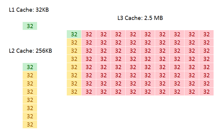
Inclusive Caches in Skylake-S: Green for L1 data, Yellow for L2 data, Red for L3 data
For Skylake-X, Intel does three things: it increases the size of the private L2 cache, which increases the hit rate for loading data, from 256 KB per core to 1 MB per core. To compensate for the increase in die area, Intel reduced the size of the size of the L3 from 2.5 MB per core to 1.375 MB per core, keeping the overall L2+L3 constant. The third element is inclusivity of the L3 cache: with it only being 1.375 MB per core, it no longer made sense for it to also hold 1 MB of the L2 data, and so with Skylake-X the L3 cache is now a non-inclusive cache (basically an exclusive cache) with the inability to obtain pre-fetch data from DRAM.
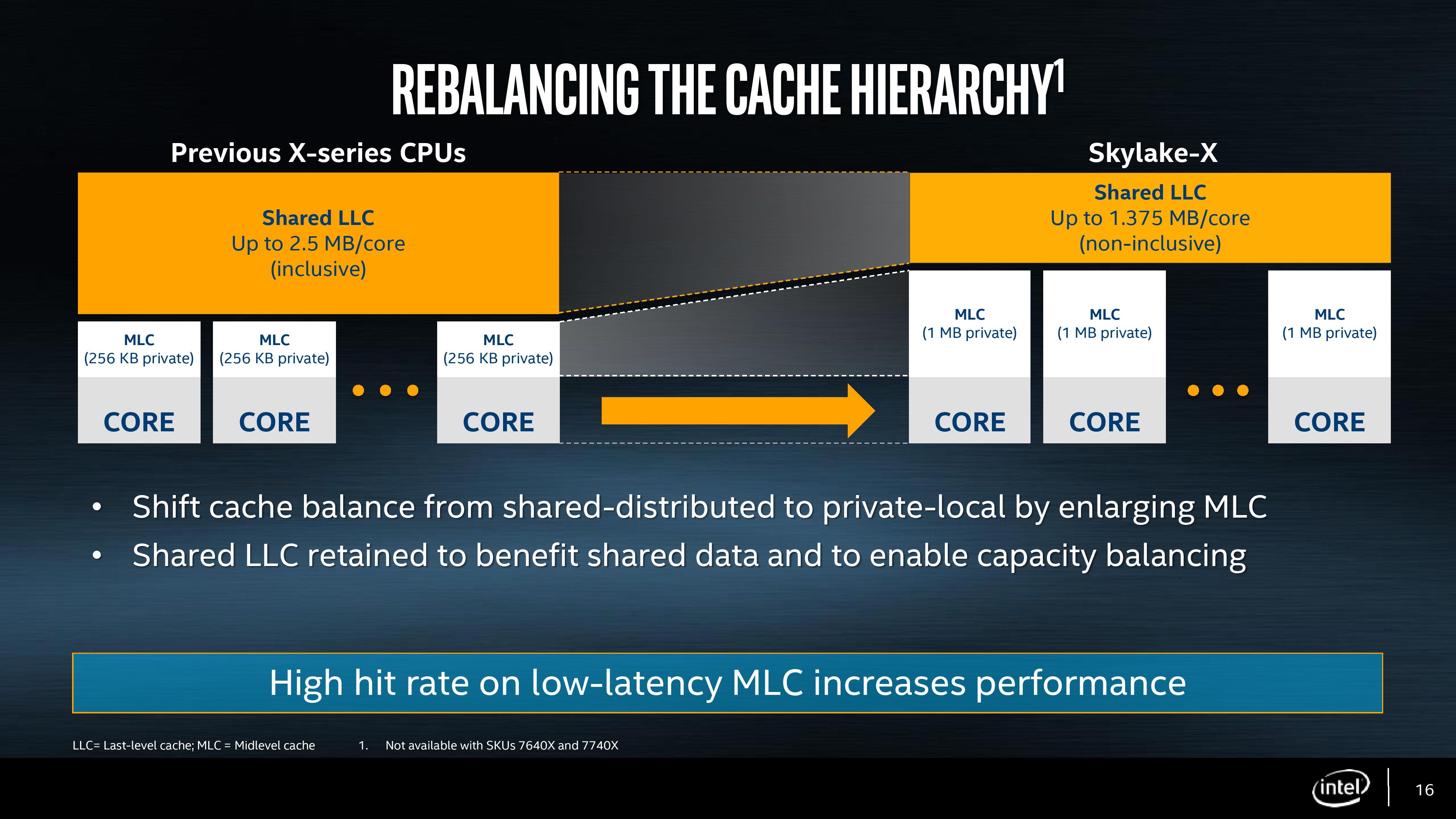
Moving the L3 to a non-inclusive cache with the inability to obtain data direct from DRAM turns it into what is known as a victim cache. When data comes in from DRAM into the L2, is used and then retired/overwritten, a copy is moved into the L3 (the L3 obtains the ‘victim’ cache line). If the data is then needed again in quick succession, there will be a copy in L3 rather than moving all the way out into DRAM. This situation depends highly on the software being used: software that has a large L2 cache requirement (e.g. 2MB) but frequency reuses data can take advantage of this scenario. Unfortunately not a lot of software is like this, and the L3 cache can become almost a dead-weight. Historically we see victim caches perform best with software that has a memory-speed bottleneck, or with integrated graphics. Skylake-X has no integrated graphics.
The upside is the size of the L2 private cache. Having spoken with engineers from different companies, a doubling of the size of the L2 cache often leads to a 1.414x decrease in cache misses (when data is not present and has to move out to the next level of cache). So by increasing the cache from 256 KB to 1 MB, thereby doubling the cache and doubling it again, the cache miss rate should be halved in total, leading to what most engineers would consider a 4-10% general IPC increase. The downside of a larger cache is that it takes longer to process data from it, adding latency. Keeping the latency low is difficult, but Intel claims that it has spent a lot of R&D effort here, with the L2 latency only moving from 11 cycles in Skylake-S to 13 cycles in Skylake-X. This will have a slight knock on that 4-10% IPC increase, but it does provide an overall benefit in almost all scenarios.
Making a Mesh: Replacing Rings with Routers
When reading about high performance processors, one phrase will always crop up: ‘feeding the beast’. In order for a CPU core to run at peak throughput, it has to continually have data to work on – if it does not have data to work on, it will sit idle and the throughput will drop. A lot of the core design is devoted to this problem: multi-level caches can store megabytes of data ready to go, and each generation brings a smarter pre-fetch engine to pull the right data from memory into cache at the right time. We’ve spoken about caches, but when a core needs data from the cache of another core, or needs to send/receive data from main memory, this also becomes a very important element to the design.
Most almost all of Intel’s processors, except for Xeon Phi, the solution to this problem has been bidirectional rings connecting the cores together (known as ring buses). The ring would allow data to travel in both directions, and it would have stations at each core (technically it grouped cores into pairs) as well as the main memory and system agent (IO). For the largest enterprise cores, in order to keep latency low, Intel separated the cores into two sets with some overlap, and a ring in each that had stations which could communicate with each other. As long as the cores and software kept the data it needed close by, latency was fairly low, and successive generations had led to higher frequencies and optimized design. The downside of a ring is scalability: the more cores you put in, the more variable the latency and more inconsistent performance can occur.

A dual ring design with Intel’s Xeon E5 v4 24-core processors
With Skylake-X, Intel felt that the ring strategy was not the right solution, and implemented its Xeon Phi strategy instead.
Rather than each core being a station on a ring, each core becomes a node in a two-dimensional grid or ‘mesh’. The node acts like a router: it is connected to the core above, the core below, and the core either side, and can direct data in each direction or drop it off at the core the node is on, similar to how a router works. In the scientific literature, this is seen as a decoupled crossbar (a central routing block), with the ‘decoupled’ bit being that every core acts like a localized crossbar.
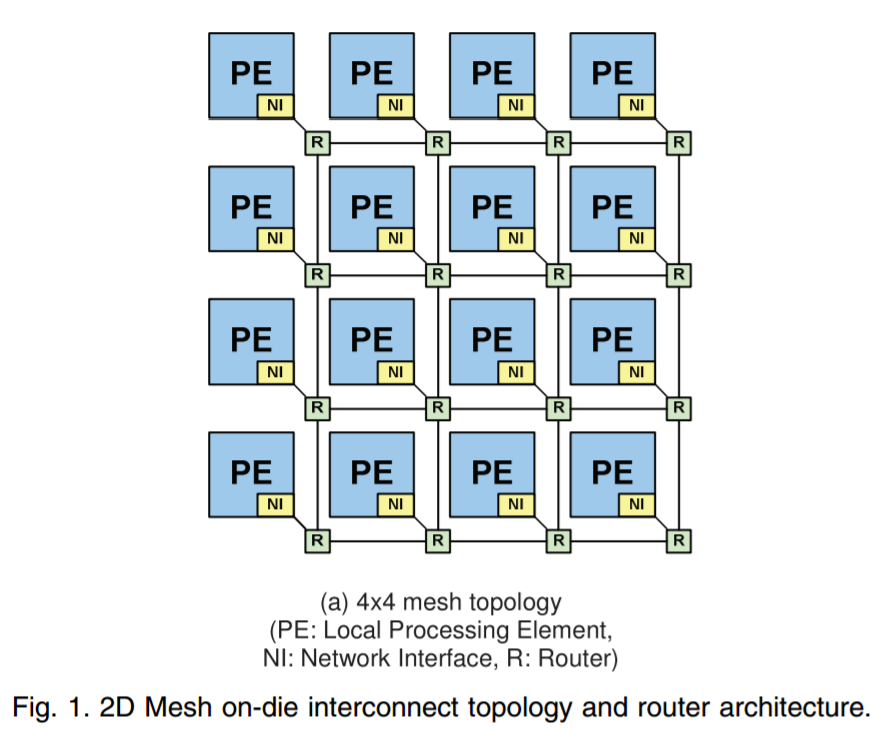
We believe that Intel is using a design known as MoDe-X, which simplifies the router at each stage to a very small routing mechanism, optimized through wiring lengths as these designs can burn power proportional to wire length. By optimizing in this way, Intel wants to reserve the power more for cores and IO. We go into greater depth on how MoDe-X works in our initial Skylake-X review.
So far the reaction to the mesh method has been mixed. While it offers scalability over using rings, it has not had over a decade of optimization, and some users have pointed to the frequency (usually 2.4 GHz) as being a bottleneck in their software over the faster ring design. Intel is likely to continue with the mesh design for the next few generations, so it will be interesting to see what upgrades are made (if disclosed).
I’ve Got 512 Problems but AVX Ain’t One: Accelerating Compute
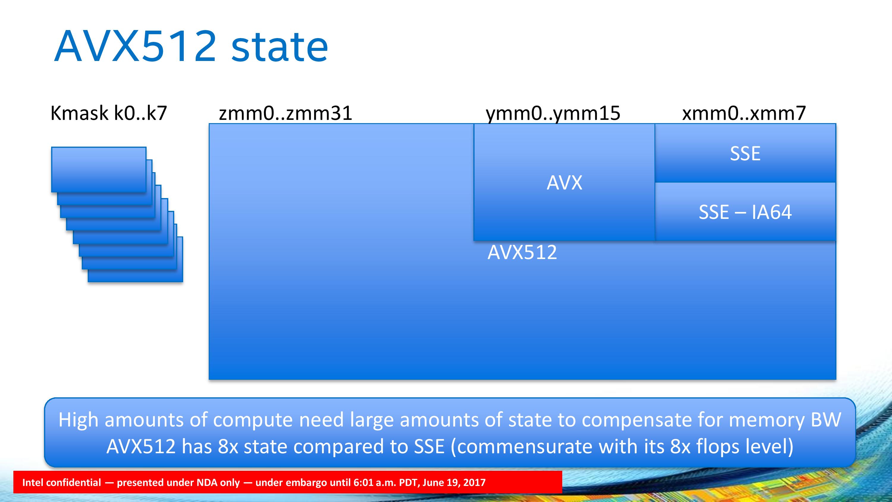
Both the cache adjustment and the mesh networking are redesigns of features already implemented in the core. AVX-512 by contrast is a distinct addition to the design, requiring a fairly substantial amount of die area (approx. 20% of a Skylake-S core). Much like AVX and AVX2 before it, the point of AVX-512 is bundling sets of data together and performing the same operation on all the data with one instruction, rather than eight or sixteen instructions.
Bundling data together to unify a single instruction is at the heart of many dense compute tasks, and most prosumer and enterprise software with high compute requirements is designed with using instructions like this to accelerate performance. Most professional software today will take advantage of AVX or AVX2 instructions, with Intel expecting the same companies to update their software with AVX512 support soon.
Due to the density of the computation, the localized energy consumption is often very high (higher than in the standard core logic), and draws a lot of power – to compensate the core will often run at a lower frequency when these instructions are used, but there is an overall net gain. The support of AVX-512 is meant to be a highlight of Intel’s enterprise processors, but due to the unified design between enterprise and HEDT, consumers are able to take advantage as well, as long as their software does. For anyone using these new processors for light tasks, or gaming, are unlikely to see any advantage through AVX-512, announcing for a lot of unused silicon on the shiny new processor.
For the new processors launched today, all of them will support dual 512-bit FMA execution through a single 512-bit FMA on port 5, and a two joined 256-bit FMAs on ports 0 and 1. Intel had noted that the six and eight core parts on Skylake-X were manufactured with the port 5 FMA disabled, however several outlets have reported that both FMAs are detected for these parts.
There is a lot to dissect with AVX-512, such as the different instruction support as well as a few new (to Intel) implementations such as mask registers and small-datatype support. We covered this in detail in our initial Skylake-X review.


152 Comments
View All Comments
ddriver - Monday, September 25, 2017 - link
You are living in a world of mainstream TV functional BS.Quantum computing will never replace computers as we know and use them. QC is very good at a very few tasks, which classical computers are notoriously bad at. The same goes vice versa - QC suck for regular computing tasks.
Which is OK, because we already have enough single thread performance. And all the truly demanding tasks that require more performance due to their time staking nature scale very well, often perfectly, with the addition of cores, or even nodes in a cluster mode.
There might be some wiggle room in terms of process and material, but I am not overly optimistic seeing how we are already hitting the limits on silicon and there is no actual progress made on superior alternatives. Are they like gonna wait until they hit the wall to make something happen?
At any rate, in 30 years, we'd be far more concerned with surviving war, drought and starvation than with computing. A problem that "solves itself" ;)
SharpEars - Monday, September 25, 2017 - link
You are absolutely correct regarding quantum computing and it is photonic computing that we should be looking towards.Notmyusualid - Monday, September 25, 2017 - link
@ SharpEarsYes, as alluded to by IEEE. But I've not looked at it in a couple of years or so, and I think they were still struggling with an optical DRAM of sorts.
Gothmoth - Monday, September 25, 2017 - link
and what have they done for the past 6 years?i am glad that i get more cores instead of 5-10% performance per generation.
Krysto - Monday, September 25, 2017 - link
The would if they could. Improvements in IPC have been negligible since Ivy Bridge.kuruk - Monday, September 25, 2017 - link
Can you add Monero(Cryptonight) performance? Since Cryptonight requires at least 2MB of L3 cache per core for best performance, it would be nice to see how these compare to Threadripper.evilpaul666 - Monday, September 25, 2017 - link
I'd really like it if Enthusiast ECC RAM was a thing.I used to always run ECC on Athlons back in the Pentium III/4 days.Now with 32-128x more memory that's running 30x faster it doesn't seem like it would be a bad thing to have...
someonesomewherelse - Saturday, October 14, 2017 - link
It is. Buy AMD.IGTrading - Monday, September 25, 2017 - link
I think we're being to kind on Intel.Despite the article clearly mentioning it in a proper and professional way, the calm tone of the conclusion seem to legitimize and make it acceptable that Intel basically deceives its customers and ships a CPU that consumes almost 16% more power than its stated TDP.
THIS IS UNACCEPTABLE and UNPROFESSIONAL from Intel.
I'm not "shouting" this :) , but I'm trying to underline this fact by putting it in caps.
People could burn their systems if they design workstations and use cooling solutions for 165W TDP.
If AMD would have done anything remotely similar, we would have seen titles like "AMD's CPU can fry eggs / system killer / motherboard breaker" and so on ...
On the other hand, when Intel does this, it is silently, calmly and professionally deemed acceptable.
It is my view that such a thing is not acceptable and these products should be banned from the market UNTIL Intel corrects its documentation or the power consumption.
The i7960X fits perfectly in its TDP of 165W, how come i7980X is allowed to run wild and consume 16% more ?!
This is similar with the way people accepted every crapping design and driver fail from nVIDIA, even DEAD GPUs while complaining about AMD's "bad drivers" that never destroyed a video card like nVIDIA did. See link : https://www.youtube.com/watch?v=dE-YM_3YBm0
This is not cutting Intel "some slack" this is accepting shit, lies and mockery and paing 2000 USD for it.
For 2000$ I expect the CPU to run like a Bentley for life, not like modded Mustang which will blow up if you expect it to work as reliably as a stock model.
whatevs - Monday, September 25, 2017 - link
What a load of ignorance. Intel tdp is *average* power at *base* clocks, uses more power at all core turbo clocks here. Disable turbo if that's too much power for you.