TechInsights Confirms Apple’s A10X SoC Is TSMC 10nm FF; 96.4mm2 Die Size
by Ryan Smith on June 29, 2017 11:30 PM EST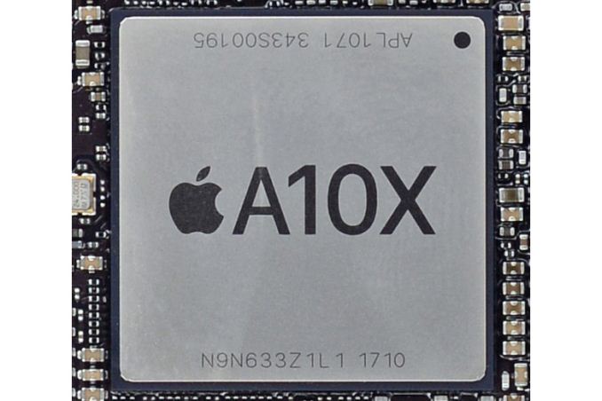
One of the more intriguing mysteries in the Apple ecosystem has been the question over what process the company would use for the A10X SoC, which is being used in the newly launched 2017 iPad Pro family. Whereas the A10 used in the iPhone was much too early to use anything but 16nm/14nm, the iPad Pro and A10X is coming in the middle of the transition point for high-end SoCs. 16nm is still a high performance process, but if a company pushes the envelope, 10nm is available. So what would Apple do?
The answer, as it turns out, is that they’ve opted to push the envelope. The intrepid crew over at TechInsights has finally dissected an A10X and posted their findings, giving us our first in-depth look at the SoC. Most importantly then, TechInsights is confirming that the chip has been fabbed on TSMC’s new 10nm FinFET process. In fact, the A10X is the first TSMC 10nm chip to show up in a consumer device, a very interesting turn of events since that wasn’t what various production roadmaps called for (that honor would have gone to MediaTek’s Helio X30)
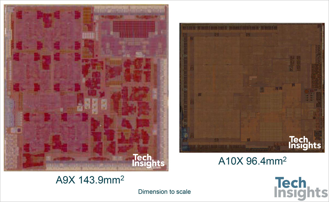
Image Courtesy TechInsights
Apple is of course known for pushing the envelope on chip design and fabrication; they have the resources to take risks, and the profit margins to cover them should they not pan out. Still, that the A10X is the first 10nm SoC is an especially interesting development because it’s such a high-end part. Traditionally, smaller and cheaper parts are the first out the door as these are less impacted by the inevitable yield and capacity challenges of an early manufacturing node. Instead, Apple seems to have gone relatively big with what amounts to their 10nm pipecleaner part.
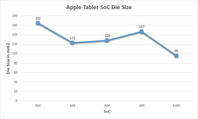
I say “relatively big” here because while the A10X is a powerful part, and big for a 10nm SoC, in terms of absolute die size it’s not all that big of a chip. In fact by Apple X-series SoC standards, it’s downright small: just 96.4mm2. This is 24% smaller than the 16nm A10 SoC (125mm2), and in fact is even 9% smaller than the A9 SoC (104.5mm2). So not only is it smaller than any of Apple’s 16nm SoCs, but it’s also about 20% smaller than the next-smaller X-series SoC, the A6X. Or, if you want to compare it to the previous A9X, Apple’s achieved a 34% reduction in die size. In other words, Apple has never made an iPad SoC this small before.
One key difference here however is that the X-series SoCs have never before been the leading part for a new process node. It has always been iPhone SoCs that have lead the charge – A9 at 16nm, A8 at 20nm, A7 at 28nm, etc. This does mean that as a pipecleaner part, Apple does need to be especially mindful of the risks. If an X-series SoC is to lead the charge for the 10nm generation, then it can’t be allowed to be too big. Not that this has stopped Apple from packing in three CPU cores and a 12-cluster GPU design.
Speaking of size, TechInsights’ estimates for area scaling are quite interesting. Based on their accounting, they believe that Apple has achieved a 45% reduction in feature size versus 16nm, which is consistent with a full node’s improvement. This is consistent with TSMC’s earlier statements, but given the challenges involved in bringing newer processes to market, it’s none the less exciting to actually see it happening. For chip vendors designing products against 10nm and its 7nm sibling, this is good news, as small die sizes are the rule for pretty much everyone besides Apple.
A10X Architecture: A10 Enlarged
Diving a bit deeper, perhaps the biggest reason that A10X is as small as it is, is that Apple seems to have opted to be conservative with its design. Which again, for a pipecleaner part, is what you’d want to do.
| Apple SoC Comparison | ||||||
| A10X | A9X | A8X | A6X | |||
| CPU | 3x Fusion (Hurricane + Zephyr) |
2x Twister | 3x Typhoon | 2x Swift | ||
| CPU Clockspeed | ~2.36GHz | 2.26GHz | 1.5GHz | 1.3GHz | ||
| GPU | 12 Cluster GPU | PVR 12 Cluster Series7 | Apple/PVR GXA6850 | PVR SGX554 MP4 | ||
| Typical RAM | 4GB LPDDR4 | 4GB LPDDR4 | 2GB LPDDR3 | 1GB LPDDR2 | ||
| Memory Bus Width | 128-bit | 128-bit | 128-bit | 128-bit | ||
| Memory Bandwidth | TBD | 51.2GB/sec | 25.6GB/sec | 17.1GB/sec | ||
| L2 Cache | 8MB | 3MB | 2MB | 1MB | ||
| L3 Cache | None | None | 4MB | N/A | ||
| Manufacturing Process | TSMC 10nm FinFET | TSMC 16nm FinFET | TSMC 20nm | Samsung 32nm | ||
We know from Apple’s official specifications that the A10X has 3 Fusion CPU core pairs, up from 2 pairs on A10, and 2 Twister CPU cores on A9X, all with 8MB of L2 cache tied to the CPU. Meanwhile the GPU in A10X is relatively unchanged; A9X shipped with a 12 cluster GPU design, and so does A10X. This means that Apple hasn’t invested their die space gains from 10nm in much of the way of additional hardware. To be sure, it’s not just a smaller A9X, but it’s also not the same kind of generational leap that we saw from A8X to A9X or similar iterations.
Unfortunately TechInsights’ public die shot release isn’t quite big enough or clean enough to draw a detailed floorplan from, but at a very high level we can make out the 12 GPU clusters on the left, along with the CPU cores to the right. Significantly, there aren’t any real surprises here. TechInsights heavily compares it to the A9X and there’s good reason to do so. IP blocks have been updated, but the only major change is the CPU cores, and those don’t take up a lot of die space relative to the GPU cores. This is what allows A10X to be more powerful than A9X while enjoying such a significant die size decrease.
As for the GPU in particular, Apple these days is no longer officially specifying whether they’re using Imagination’s PowerVR architecture in their chips. Furthermore we know that Apple is developing their own GPU, independent from Imagination’s designs, and that it will be rolled out sooner than later. With that said, even prior to today’s die shot release it’s been rather clear that A10X is not that GPU, and the die shot further proves that.
Apple’s developer documentation has lumped in the A10X’s GPU with the rest of the iOS GPU Family 3, which comprises all of the A9 and A10 family SoCs. So from a feature-set perspective, A10X’s GPU isn’t bringing anything new to the table. As for the die shot, as TechInsights correctly notes, the GPU clusters in the A10X look almost exactly like the A9X’s clusters (and the A10’s, for that matter), further indicating it’s the same base design.
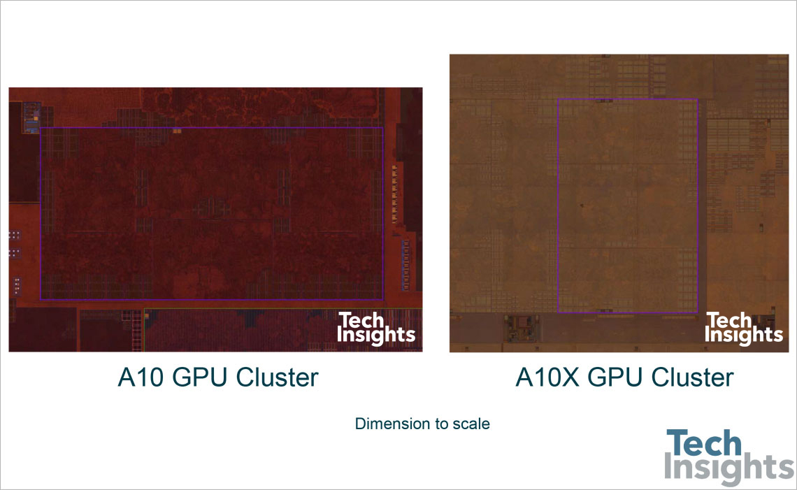
Image Courtesy TechInsights
Ultimately what this means is that in terms of design and features, A10X is relatively straightforward. It’s a proper pipecleaner product for a new process, and one that is geared to take full advantage of the die space savings as opposed to spending those savings on new features/transistors.
Otherwise I am very curious as to just what this means for power consumption – is Apple gaining much there, or is it all area gains? A10X's CPU clockspeed is only marginally higher than A9X's, and pretty much identical to A10, so we can see that Apple hasn't gained much in the way of clockspeeds. So does that mean that Apple instead invested any process-related gains in reducing power consumption, or, as some theories go, has 10nm not significantly improved on power consumption versus 16nm? But the answer to that will have to wait for another day.
Source: Capped A10X Photo Courtesy iFixit


87 Comments
View All Comments
Kevin G - Friday, June 30, 2017 - link
This makes me wonder what they have in store for the A11 in the next iPhone due later this year. I think this sets up the expectation that Apple will use 10 nm there as well. I'd still expect a dual big + dual little design. The change maybe that Apple could enable all four cores simultaneously under heavy load. More cache as we've seen on the A10X is probably a given, I'd guess 6 MB. GPU side is where I'd see the big changes happening for the A11 with a new cluster design. I don't think they'll have their custom GPU ready by then but Apple has been known to surprise. I see Apple adopting the latest PowerVR design and increasing the cluster count.name99 - Friday, June 30, 2017 - link
"I'd still expect a dual big + dual little design."This is not a useful way to look at it; it reflects ARM thinking, not Apple thinking.
Apple, as far as we can tell, does not design of think of these as "dual big" and "dual little", they think of them as a "flexi-core" that consists of a big and a little very tightly coupled. The difference is that the unit of construction is the "big+little" it's not clusters of big and clusters of little.
We appear to know that switching between a big and its companion little is done by HW. (Apple talks about a "HW performance controller" doing this job). It also seems to be the case that the two can't run independently (big and little running simultaneously) though it's not clear if this is a HW limitation, an OS limitation, or just a policy decision (Apple experimented and could find no circumstances under which it really made sense).
If I had to bet, my betting would be that as we move forward the big and little cores will become ever closer, ever more like two sides of a single "flexicore", so perhaps even moving to sharing L1 cache for example. We'll see...
(ARM has STARTED down this path with DynamIQ --- at least now big and little cores can have a tighter association rather than being forced into separate clusters using separate L2s. Not clear yet if DynamIQ allows for HW to control the toggling between big and little rather than software.)
Kevin G - Friday, June 30, 2017 - link
I'm not disagreeing with you but there isn't much in terms of terminology to quickly describe that arrangement. It is an implementation distinctly different from what ARM is doing but they both do the same thing at a high level.Sharing L1 cache would be nice as swapping between the two designs wouldn't haven't move data for warming caches. However, I can it being difficult to keep L1 latencies low in such a scenario Perhaps just a shared L1 data cache and dedicated L2 instruction caches?
kfishy - Friday, June 30, 2017 - link
Heck, since it's on the same silicon and using the same process you can theoretically even share the registers and just swap the big/little pipelines and execution units.name99 - Friday, June 30, 2017 - link
One problem is that you want the little core not just to have a simpler micro-architecture but ALSO to be built of slower transistors. That reality would seem to constrain how aggressively you can push sharing.But there are academic designs (Univ North Carolina Chapel Hill has done a lot work in this) that share almost everything and do the big/little transition by shutting down parts of the big microarchitecture. They utilize counters to predict regions of code that will not benefit from the wide micro-architecture (maybe lots of misses to memory, maybe lots of sequentially dependent instructions, maybe lots of hard to predict misses), and switch between the wide and the more narrow configs at around every thousand instructions or so. In theory these give substantial energy savings at a performance loss of 3..5% (which you can easily make up and more just by cranking the frequency higher).
But I'm guessing it will be some time before the commercial world gets there! Let's see if they're at least headed that way by seeing whether Apple's next config pulls the two CPUs tighter together.
kfishy - Sunday, July 2, 2017 - link
Oh yeah, slower less leaky transistors definitely help, but even just switching fewer transistors with a simpler pipeline would yield non-trivial power savings.iwod - Friday, June 30, 2017 - link
Actually this got me thinking may be there wont be A11. Apple will use the same A10X for iPhone 8. Since 10nm is a short node, it is only a stepping stone to 7nm. May be the innovation, Apple made GPU, new CPU architecture, will only come next year?Nullify - Friday, June 30, 2017 - link
Now where are Samsung and Qualcomm with their higher end SoCs for tablet use? Seems ridiculous to use the same one as your phone when a tablet is where you want to extra power.Araa - Friday, June 30, 2017 - link
The thing is they don't have anything better than what they put in their phones.blackcrayon - Friday, June 30, 2017 - link
Seems like Apple is the only one with the profit margin and tablet sales to justify developing customized higher end chips. For Samsung their high end phone chips are "good enough". Of course Apple does this too but only in their lower end tablets at this point (lone exception was the iPad Air).